

By now, we’ve all heard about the Artificial Intelligence (AI) surge that is going to demand unprecedented amounts of energy. Even the International Energy Agency (IEA) released a report on Energy and AI recently. The advanced energy materials that are the foundation of these digital solutions are semiconductors.
Semiconductors and AI Linked by a Highly Complex Supply Chain
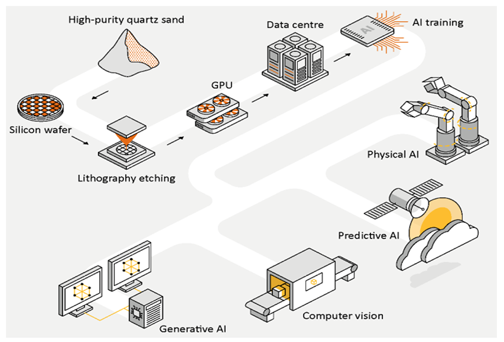
Source: International Energy Agency, 2025
What are Semiconductors?
Do you imagine that electricity flows through power cables like water flowing through a pipe? It doesn’t. The electricity is always there and accessible through nodes, e.g., your home’s power outlets, that are like gates that open and close according to when you need power. Electrons flow freely through conducting materials when those gates are open to deliver power to your electric vehicle, for example.
Similarly, semiconductors can be thought of as having gates that open and close, allowing electrons to flow and create circuits. Semiconductors are primarily built on silicon, an abundant and efficient material. These are building blocks that form transistors and other components that are then integrated into complex circuits on chips. Those chips form the core components that deliver computers, AI, and other digital solutions we all know.
Semiconductors Enable Cleantech, But Production Emits Carbon
Despite the tiny nature of semiconductors, manufacturing consumes a lot of time, money, and resources. Building a single fab can cost upwards of $25B due to the complex manufacturing processes that are comprised of hundreds of steps, over fifty types of equipment, and highly specialized labor. A new fab in the U.S. and Europe takes twice as long to design and construct and costs twice as much than in Taiwan.
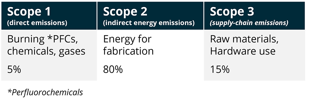
From a sustainability point of view, manufacturing semiconductors is incredibly resource intensive. Toxic ‘forever chemicals’ (fluorinated chemicals/PFAS) make up nearly 90% of direct emissions (Scope 1), mostly used for cleaning. But replacing these chemicals could still be 5-10 years away and non-PFAS alternatives are 20+ years away.
Electricity is the single biggest source of emissions (Scope 2)—60% for manufacturing; 40% for operation of facilities. On the supply side (Scope 3 emissions), utilization of new materials does not significantly impact the overall industrywide emissions profile. Scope 3 emissions are mainly attributed to mining and refining from outside of the industry. Forward looking, global emissions will rise 8% annually, doubling by 2045 from 2023 (SEMI, BCG, The Semiconductor Climate Consortium).
Water usage is another area of opportunity for innovation. Manufacturing a single chip requires 8,327 L of ultra-pure water, and a single fab will consume upwards of 25M-35M L daily. In Taiwan, fabs will recycle 80% of water usage, but in most other countries only 10% or less is recycled. From 2021-2024, Micron and Aqua Membranes were developing technology to recycle water usage. After successful trials, the two are committed to recycling 95% of Micron’s water usage by 2030.
Key Innovations – Design, Photonics, and Compound Materials
No single breakthrough innovation is catapulting the industry forward from a sustainability point of view, but there are a number of exciting areas to pay attention to.
Design – Intellectual Property (IP) Reuse
IP reuse and discovery is primarily done manually by engineers, but digital solutions are coming online breaking through the historically cost-prohibitive barriers that kept many fabs from uptake.
![]()
Thalia is a provider of a software platform that enables semiconductor businesses to develop new products using existing chip designs for analog. Thalia leverages AI/ML to mine data for IP reuse to streamline design to fabrication. This automation leads to reduced cycle time and costs for its customers and ultimately improved component reliability.
Design – Materials
The individual wafers may be designed with compounds like gallium nitride or indium phosphide. These may have efficiency increases and may result in carbon emissions reductions at smaller scales.

PseudolithIC is a manufacturer of hybrid semiconductor products which integrate compound semiconductor chiplets into silicon wafers. These compound chiplets combine the energy capacity of high energy materials (compound III-V) like gallium, indium, etc., with silicon. This maximizes performance while reducing manufacturing costs. It’s targeting the RF market with defense and telecom markets leading in demand.
Fabrication – Photonic Integrated Circuits (PICs)
PICs use light (photons) rather than electricity to process information. This translates into energy waste reduction for faster and more efficient data handling. While not projected to scale in the 2030s, PICs do represent significant energy savings potential. It’s thought that PICs will have an impact similar to the microelectronics revolution in the 1980s. PICs could deliver products that are an order of magnitude faster than today’s electronics.
![]() NXP Semiconductor backed Smart Photonics is a manufacturer of indium phosphide (InP) semiconductors for PICs. Smart Photonics recently partnered with X-Fab and Epiphany Design to demonstrate InP-on-Silicon for optical transceivers. It intends to target datacenters, sensing, and telecom.
NXP Semiconductor backed Smart Photonics is a manufacturer of indium phosphide (InP) semiconductors for PICs. Smart Photonics recently partnered with X-Fab and Epiphany Design to demonstrate InP-on-Silicon for optical transceivers. It intends to target datacenters, sensing, and telecom.
Metrology
Quality control, process optimization, and testing software and equipment keep contaminates out for high precision manufacturing.
![]() Wooptix is a manufacturer of semiconductor metrology equipment incorporating wavefront phase imaging (optics) for non-invasive sensing to ensure that each component meets stringent quality standards.
Wooptix is a manufacturer of semiconductor metrology equipment incorporating wavefront phase imaging (optics) for non-invasive sensing to ensure that each component meets stringent quality standards.
![]() K2 Photonics developed a single cavity dual-comb laser for metrology for semiconductor inspection. This provides rapid and precise thin-film inspection.
K2 Photonics developed a single cavity dual-comb laser for metrology for semiconductor inspection. This provides rapid and precise thin-film inspection.
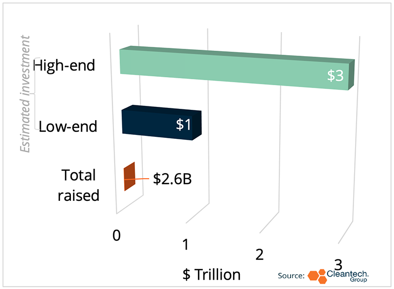
$2.6B Total VC Funding for Semiconductors from 2020-2024:
Far from $1T-$3T Needed by 2030
Geopolitical Tensions, Rising Costs, Undeveloped Supply Chains
The opportunity to bolster AI and datacenters, among many other cleantech applications, is threatened by the semiconductor industry’s concentration in Taiwan. Vulnerabilities within the supply chain are further exacerbated by geopolitical tensions like the U.S.’ 32% tariffs imposed on exports from Taiwan. We’ve seen significant funding by the public sector like the $53B U.S. Chips & Science Act or the $47B EU Chips Act.
But these investments have not resulted in any significant breakthrough technological advancements yet, especially in Europe and China. Countries are pressuring incumbents to expand business outside of Taiwan, but incumbents are pushing back, calling on policymakers to provide financial incentives, e.g., subsidies for materials. Still, the current project pipeline is booming, particularly for the U.S. that has committed over $540B in supply chain investments since 2020 via grants, loans and project development:
- TSMC has invested $165B to build new fabs in the U.S.
_ - Nvidia announced a $500B plan to manufacture in Arizona in partnership with TSMC and plans to build out more fabs in Texas with Foxconn and Wistron
_ - Apple is set to invest over $500B to build new fabs in U.S., as well
From 2020-2024, we tracked over $2.6B of VC investments for semiconductor innovation. This is far from the estimated $1T-$3T worth of investment needed from 2020-2030 in R&D and capital to deliver the next generation of semiconductors (The Semiconductor Industry Association, BCG). These figures are estimated for the semiconductor industry as a whole, not just cleantech. We spent approximately this much to get us where we are today, so these figures, while large, are manageable.
Part of the reason for these large figures is the cost to build a semiconductor fab and its highly complex supply chain. Due to this complexity, no single producer country is capable of manufacturing semiconductors without sourcing some part of the supply chain from elsewhere. This presents an especially lucrative opportunity for play in this distributed supply chain to allow for quicker lead times and greater collaboration among the ecosystem.
